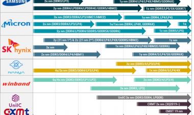
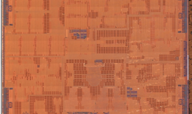
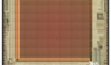
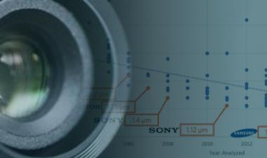
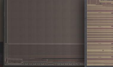
去年,三星宣布在Exynos 9825中使用的7LPP工艺中引入EUV。通过对零件的分析,我们发现9825的7LPP工艺和Exynos 9820的8LPP工艺差别不大。
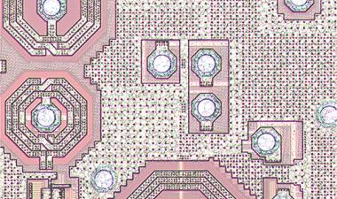
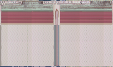
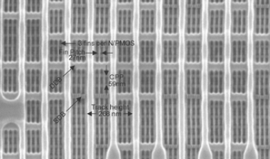
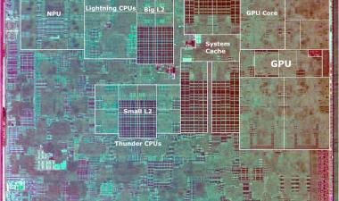
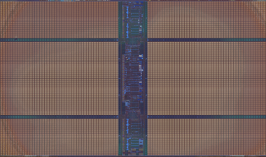
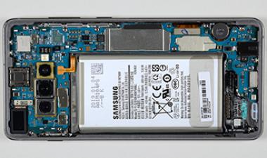
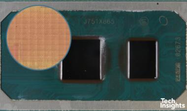
现在,我们很高兴地说,我们已经发现三星真正的7LPP过程中的Exynos 990,包括在他们的旗舰银河S20。正如我们所料,这种7nm EUV工艺提供了三星迄今为止观察到的最高密度布局。
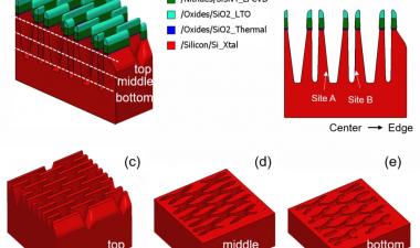
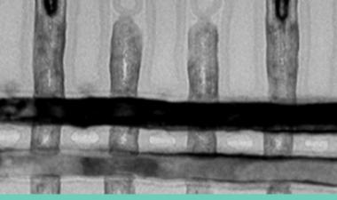
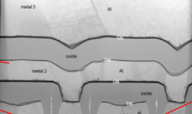
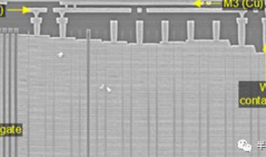
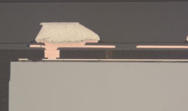
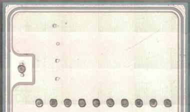
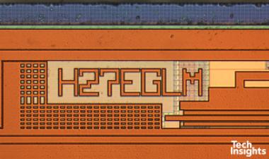
With a 27nm fin pitch, this disruptive innovation enables a smaller standard cell height of 270nm while maintaining high drive current with a 3/3-fin layout for both NMOS and PMOS transistors.
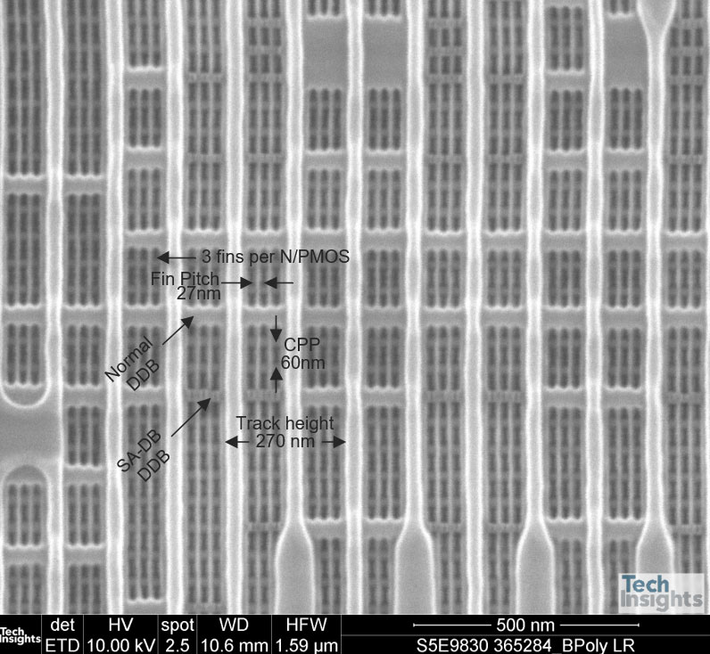
这表明与台积电N7 7.5T 3/3翅片布局(标准单元高度为300nm)和6T 2翅片布局(标准单元高度为240nm)相比,EUV光刻实现的密度增加。
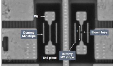
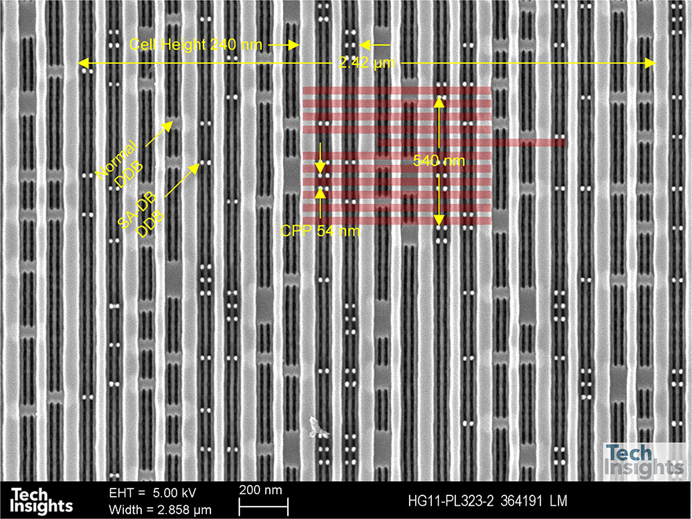
Intel’s 10nm process has a similar 272nm standard cell height, but achieved this with 2/3 fin layout. In addition to pitch scaling, in a surprise implementation, Samsung has introduced a SA-DB (Self Aligned Diffusion Break) that likely reduces performance variation caused by the local layout effect (LLE) of PMOS transistor. This is the first time we found in this device. We also started working on Snapdragon 765G fabbed by same Samsung 7LPP as Exynos 990, it turned out having new features that 243nm standard cell height with 2/2 fin layout and 54nm gate pitch. It should be comparable with TSMC N7 or N7P 2/2 fin layout high density cell.
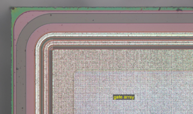
TechInsights将更仔细地检查这些部分;到目前为止,我们计划进行以下分析:
| 品名 | 产品代码 | 订阅/频道 |
|---|---|---|
| 三星Exynos 990数字功能分析报告 | DFR-2003-801型 | 逻辑-数字平面图 |
| 三星Exynos 990 aCMOS软件包 | ACE-2003-801 | 逻辑-过程 |
| Qualcomm Snapdragon 765G Digital Floorplan Analysis Report | DFR-2002-802 | 逻辑-数字平面图 |
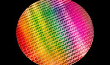
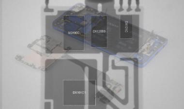
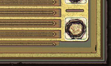
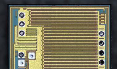
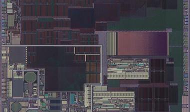
三星Exynos 990 7nm EUV工艺分析
在Samsung Exynos 990中了解有关Samsung真实7LPP进程的更多信息,我们正在进行的分析