作者:Arabinda Das
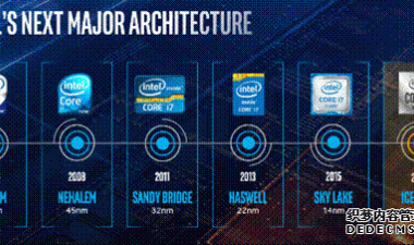
Today the semiconductor industry is a behemoth whose年销售收入跨越4000亿美元. 在其60年的历史中,这个成熟的行业已经尝试了各种模式,如集成设备制造商(IDM)、无晶圆厂(fabless)和铸造概念,每一种都采用了不同的知识产权(IP)策略。
在早期阶段,在1960年至1970年之间,设计ing an integrated circuit (IC) was a laborious task as it required specialized engineers who, without the help of electronic-design-automation (EDA) tools, had to manually create the circuits and layouts. This limited R&D to a select few manufacturers who could afford this costly process. At that time, the manufacturers had their patents centered around all aspects of their product.
在20世纪80年代早期,EDA工具开始出现在市场上,导致过程标准化,使更多的参与者能够进入制造领域。这种标准化有助于分离设计和制造过程;现在可以在一个地方设计,在另一个地方制造。这是一个巨大的解脱,因为制造变得极其昂贵,需要定期升级设备和工艺。这种分裂产生了各种分类,如IDM,无晶圆厂和铸造厂。
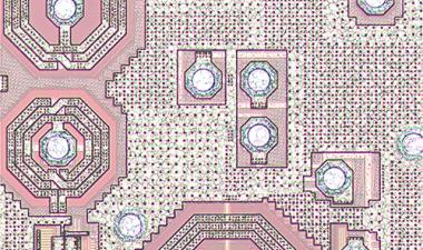
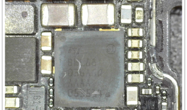
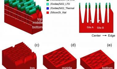
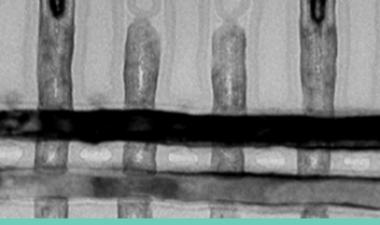
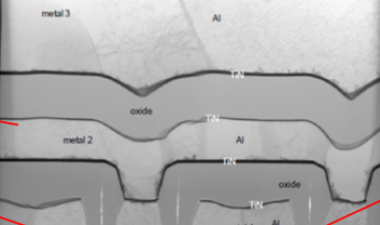
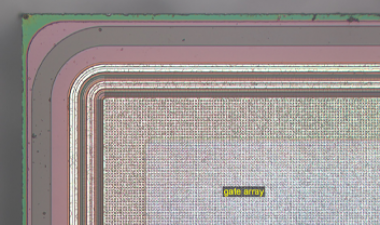
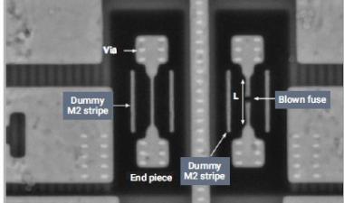
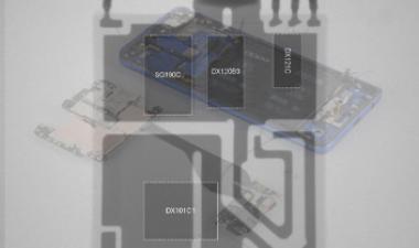
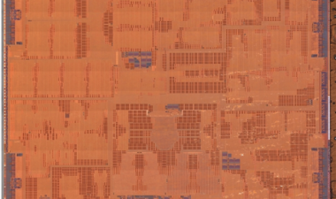
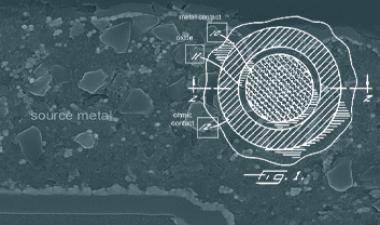
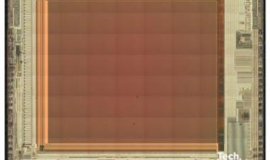
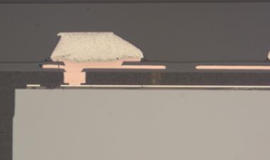
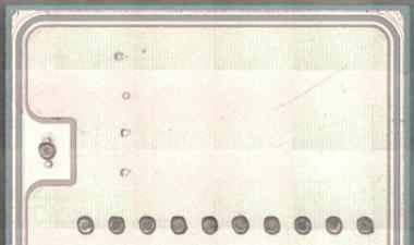
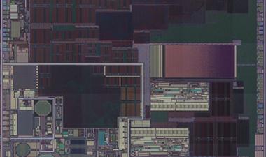
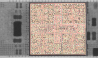
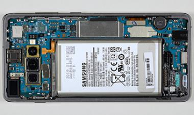
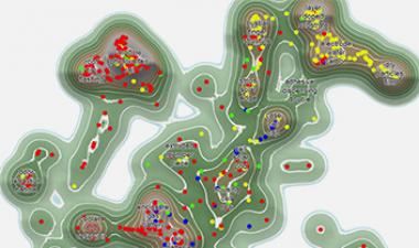
IDM包括最有资源的组织,如德州仪器、英特尔和IBM。他们有一个完整的概述,从设计阶段到产品。他们还制造了逻辑和存储设备,为他们的投资组合增加了广泛的专利。图1描绘了来自Techinsights库的1990 Texas Instruments(TI)4MB CMOS DRAM。该装置采用沟槽电容器进行数据存储。德州仪器公司不仅设计了DRAM,还制造了DRAM,并将其封装在美国自己的网站上。如今,TI不再制造任何内存产品或逻辑处理器,但他们仍在继续将其庞大的知识产权资产货币化。

图1:IDM Texas Instruments的早期DRAM(1989-1990)
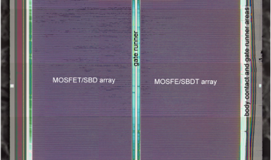
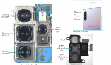
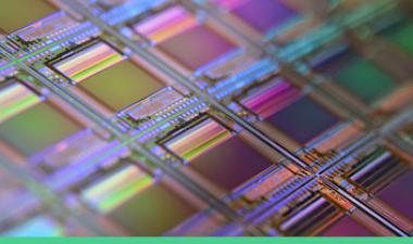
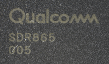
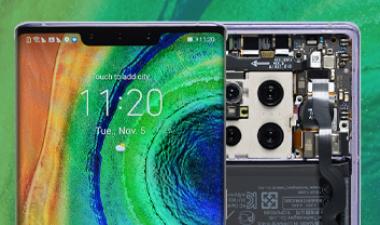
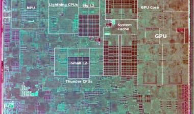
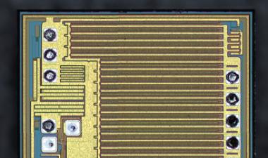
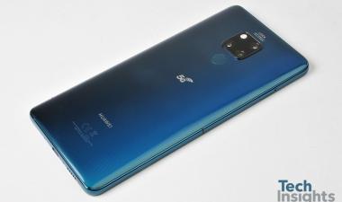
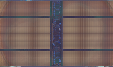
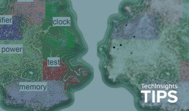
无晶圆厂模型设计自己的产品,但依赖铸造厂来制造。因此,无晶圆厂的组织只专注于其产品能够推向市场的功能和应用,并相应地申请了专利。高通公司是采用无晶圆厂模式的先驱之一,这种模式在今天仍然适用。图2的图片来自高通公司,一张是在90年代后期制作的,另一张是他们最新的设备之一;这两张图片都在Techinsights进行了分析。左边的图像有芯片标记,表明芯片是由英特尔制造的。右边的图片是三星制造的。
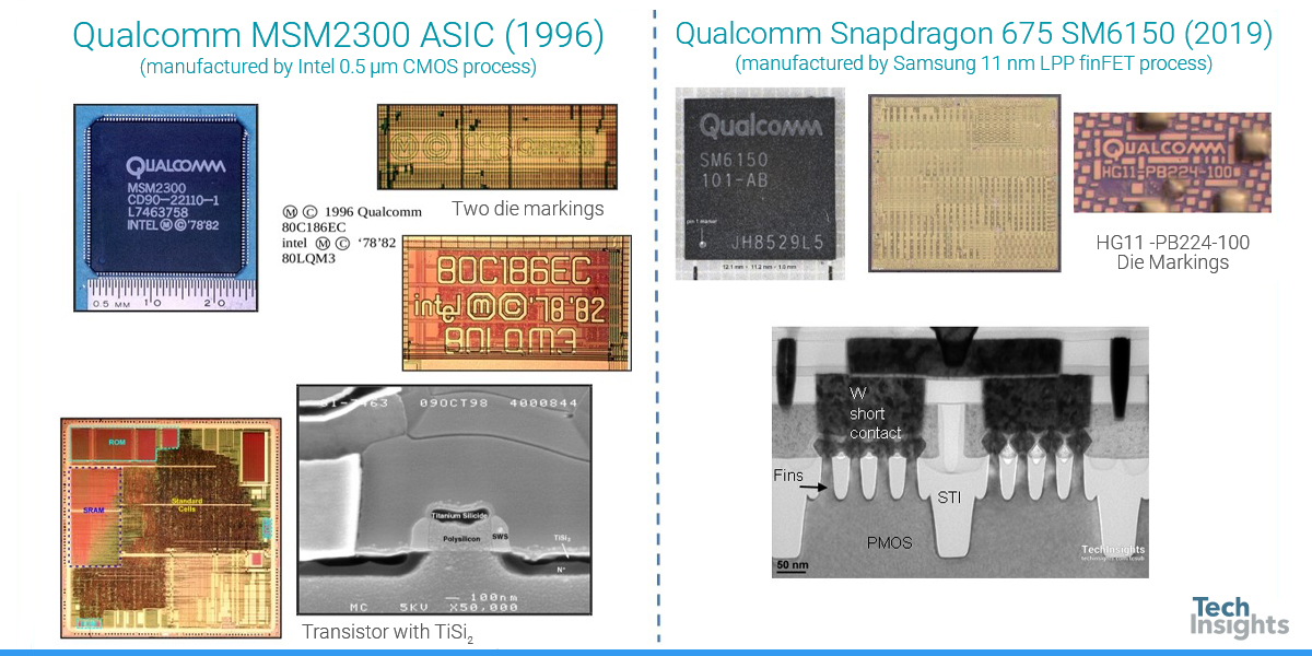
图2:来自不同时代的无晶圆厂高通公司的两台设备
铸造厂一直面临着制造方面的挑战,如缺陷密度、蚀刻选择性和高宽高比结构的填充,因此需要不断寻找解决方法。他们解决的每一个重大问题都产生了一项专利。在接下来的10年里,无晶圆厂和铸造厂的专利组合保持着明显的差异。随着时间的推移,许多IDM退出了半导体行业或采用了无晶圆厂铸造模式;维持整个半导体工艺的挑战需要巨大的资源和公平。
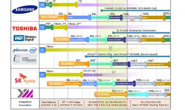
世纪之交,半导体技术领域取得了巨大的进步,包括IBM在1997年推出了铜互连,后来被所有其他逻辑制造商采用。铜互连线带来了新的挑战,如铜和钽基势垒的化学机械抛光、铜大马士革结构的错配和电迁移问题。所有这些问题都得到了解决,并产生了来自不同制造商的大量工艺专利。这一时期也经历了摩尔定律的顶峰,即每两年芯片上的晶体管数量就会翻倍,从而使得制造电子设备的成本更加低廉。在那个时期,各种各样的芯片被制造出来用于各种各样的应用。这些芯片安装在不同类型的印刷电路板上,根据输入/输出的数量,它们的配置可能会有所不同,包括引线键合、倒装芯片、引脚栅极阵列、表面贴装技术等等。这些包的配置和流程非常不同,必须由一个完全独立的组织来处理。外包装配试验(OSAT)诞生于20世纪90年代末,无晶圆厂铸造模型已经在亚洲建立了生产基地,而设计仍在美国和欧洲。OSAT将其传播范围进一步扩大到亚洲其他国家。OSAT做了一项艰巨的工作,测试设备和包装他们和专利的后端过程。人们不应忘记,几个密切关注整个过程的IDM为封装行业的许多重要里程碑做出了贡献,例如球栅阵列和倒装芯片铜柱工艺。到2000年代中期,有四个不同的集团(IDM、铸造厂、无晶圆厂和OSAT)开发了自己独特的IP。
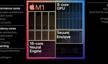
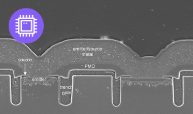
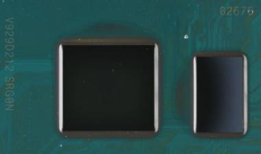
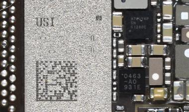
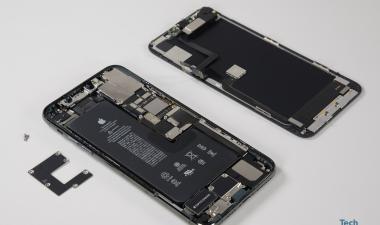
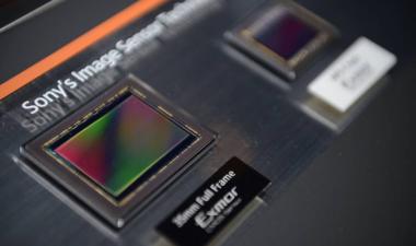
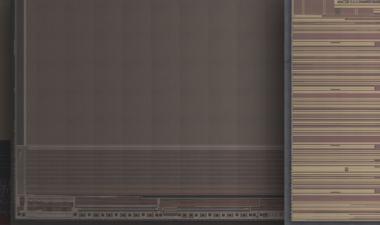
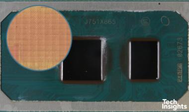
The status quo of the chip ecosystem was disrupted by the introduction of the iPhone in 2007. Smartphones assembled in a small footprint have several components like display, touch screens, cameras, microphones, speakers, battery, sensors, antenna, Wi-Fi connectivity, memory, processors, storage and more not to mention all the different types of software which exist to facilitate daily operations. As smartphones developed, it became a dire necessity to innovate new compact packages, optimize the interconnect structures between disparate devices, and provide powerful computation capabilities to processors. Smartphones connected the general public to the internet and made the transfer of large amounts of data possible, ushering in the need for better data collection and manipulation. Data organizations required application specific processors which were not yet available in the market; this demand pressured companies to meet this need. As a result, the boundary line between the design-house, the foundry, and the software companies became quite blurred: Foundries began getting involved with design and packaging. Particularly, TSMC one of the leading foundries, expanded its portfolio in a variety of fields. Today, TSMC manufactures chips for various companies including Apple and has developed its own proprietary integrated fan-out (InFO) packaging technology, in which stacked DRAM dies are placed on top of an embedded processor that has redistribution lines on its molding compound. Figure 3 shows one of the latest packaging products by TSMC, which is used mainly for Apple processors.
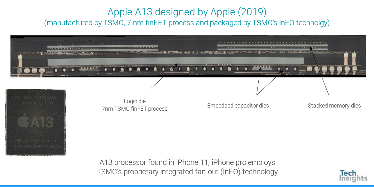
图3:集成扇出封装从铸造台积电
同样,微软、苹果和谷歌等数据公司也开始为自己的应用程序设计芯片。这创造了半导体工艺的重新整合;不同组织的融合导致了专利在投资组合的交叉点上的创造。未来,随着5G等技术的出现,各个群体的专利将有更大的混合。
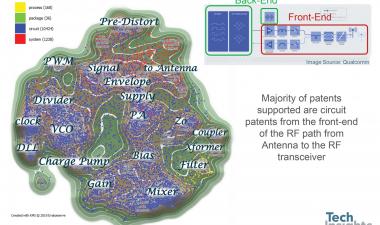
Recently, I came across a detailed landscape report on 5G, presented by Ed White from Drewent [2]. One of the main takeaways was that the inventions of top 5G assignees (Samsung, Apple, Huawei, Qualcomm, Ericsson and Nokia) could be divided into thirty-seven technical categories. These six companies possess 41% of the 5G patents and none of them have any manufacturing capacity (Samsung being the exception). Nevertheless, they all have filed patents in all sorts of technical categories including healthcare, education, agriculture, automotive, multiple access schemes, antenna, and enhanced mobile broadband. This wide portfolio suggests that it is extremely difficult to categorize a company into a single box and assign it a unique specialization. Software companies, IDMs, foundries, and fabless are all filing patents over an entire, disparate spectrum.
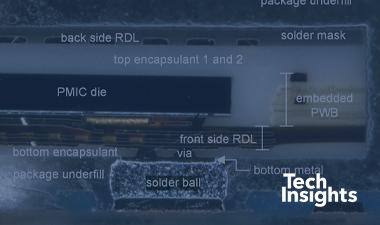
考虑到在5G时代,一些现有配置将出现新的应用,情况变得更加复杂。例如,5G的突出技术之一是大规模MIMO(多输入多输出)技术。mimo被配置成允许无线网络在单个无线信道上发射和接收多个数据信号。为了实现这一点,在同一个平台上需要多个天线;因此,未来的智能手机将拥有更复杂的天线结构。这一概念开启了一种新的封装应用,称为包内天线(AIP)或包上天线(AOP),它是嵌入式扇出封装的一个子集。嵌入式扇出式封装是为了将有源和无源器件(如天线、电感器和电容器)集成在封装中而设计的。英飞凌是嵌入式扇出封装的先驱之一,他们的嵌入式晶圆级球栅阵列(eWLB)于2008年开发,授权给STATS ChipPAC、ASE和Amkor。这三家OSAT公司通过提供解决方案,将多个有源和无源器件集成到软件包中,包括天线结构,进一步发展了最初的想法;这鼓励了许多其他参与者加入扇出技术社区。英飞凌在2019年为谷歌Pixel 4智能手机打造了一款精确的运动检测设备技术,当时他们没有使用嵌入式扇出技术。相反,they incorporated the antenna in the printed circuit board,根据Techinsights进行的结构分析得出[4,5]。这进一步强化了大多数现代科技巨头所接受的跨学科思维模式。今天,有至少有10家公司直接参与扇出晶圆级封装[3] ,其中8人是OSAT玩家。
除了明确的界限消失之外,知识产权(IP)不断易手的事实使专利格局更加复杂。据IAM编辑R.Lloydthe first quarter of 2020 saw the largest number of US patent deals and the largest amount of assets changing hands[6]. 事实上,自2010年对专利交易进行跟踪监测以来,2020年的知识产权变动幅度最大。IBM、LG和诺基亚是一些最突出的卖家,而大多数买家是非执业实体,而台积电、三星和索尼则是前五大买家。显然,半导体工业已经从DRAM专利只适用于特定产品的时代开始了。如今,这项技术仍被分割成许多专门领域,但与此同时,不同类别之间的接口比以往任何时候都更加流畅。由此产生的专利前景具有挑战性,但也充满了知识产权实践的机会。保护一个人的知识产权没有单一的战略;一个可能的前进道路是接受开放创新的概念。主要思想开放式创新是到integrate or accept ideas and technologies from an outside organization in order to enhance one’s own innovation[7]. 这使得半导体公司能够专注于自己的核心优势,并在自己不具备所需技能的领域依赖与其他公司和/或研究联盟的大规模合作。希望知识产权的未来集中于创意的出现,这正是半导体行业的特点。与此同时,Techinsights正在继续跟踪技术进步,并密切关注不断变化的专利格局。
TechInsights的存在是为了支持一个半导体和电子知识产权可以创新和货币化的公平市场。我们是世界领先的先进技术分析和知识产权服务.
参考文献:
[1] https://www.semiconductors.org/the-2020-sia-factbook-your-source-for-semiconductors-industry-data/
[2] 《在5G领域发现机遇》,作者:Ed White,IAM winter 2019
[3] https://semiengineering.com/fan-out-wars-begin/
[4] https://www.infinon.com/cms/en/about-infinon/press/press-releases/2019/INFPMM201910-003.html
[5] Infineon 6TR13C Package briefings 2019, Techinsights
[6] https://www.iam-media.com/non-practicing-entities/new-data-points-bumper-first-quarter-of-patent-deal-making
[7]关于开放式创新,你需要知道的一切
Open Innovation and Intellectual Property Rights- The Two-edged Sword