撰稿人:辛金·迪克森·沃伦
碳化硅(SiC)功率晶体管的市场在未来几年将有相当大的增长。与传统的硅基器件相比,SiC功率晶体管具有许多优点,包括在高温、高频和高压应用中性能的提高。这使得碳化硅功率晶体管非常适合汽车,能源和工业应用。随着制造商努力满足对SiC功率晶体管日益增长的需求,有必要对制造工艺进行创新,以降低成本和提高性能。最先进的技术可用于分析这些创新,并重建制造过程中使用的步骤序列。由此产生的工艺流程可以为SiC功率晶体管制造所需的设备和材料提供有价值的见解。
TechInsights最近完成了全面分析介绍了用于制造Rohm-SCT3022ALGC11 N沟道、SiC沟道、功率MOSFET的工艺流程。这个SCT3022ALGC11型是一个650伏,93安的装置DSON公司22m³。它是一个领先的蚀刻SiC沟槽门电源FET,设计用于太阳能逆变器,DC / DC转换器,开关模式电源,感应加热和电机驱动器。
我们的分析员利用他们对光刻技术的知识来选择一个用于分析的设备区域,该区域将提供对制造工艺流程的最大洞察,特别是晶体管阵列的单个单元。然后使用扫描电子显微镜(SEM)成像、能量色散x射线光谱(EDS)和扫描电容显微镜(SCM)成像等技术对该区域进行分析。由此产生的图像和数据被用来确定设备中存在的物理特征和材料。仔细分析这些特征和材料,可以创建一个表来描述包括光刻掩模在内的工艺步骤。然后将数据提交给委员会Synopsys Sentaurus进程浏览器模拟器可以全面仿真过程流程。
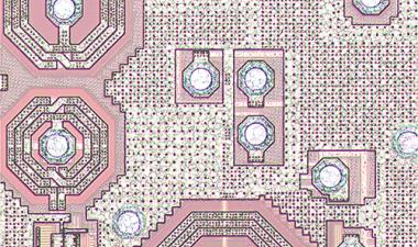
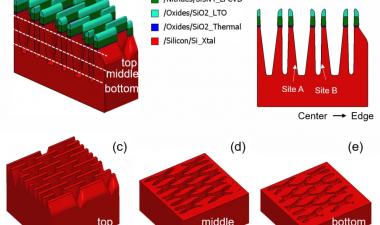
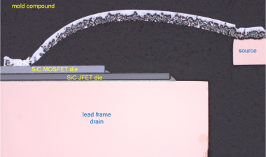
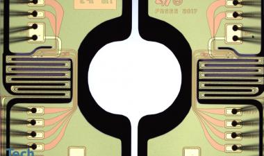
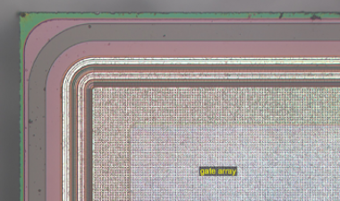
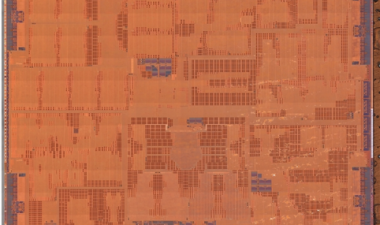
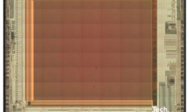
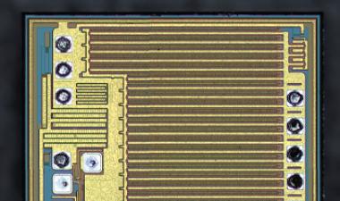
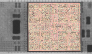
如图1所示,SIC MOSFET的角落的地形视图提供了布局信息,以帮助选择目标区域进行分析。晶体管栅极阵列包含许多重复的方形电池结构,其用于分析的示例性区域。选择其中一种细胞用于分析和最终的过程仿真。
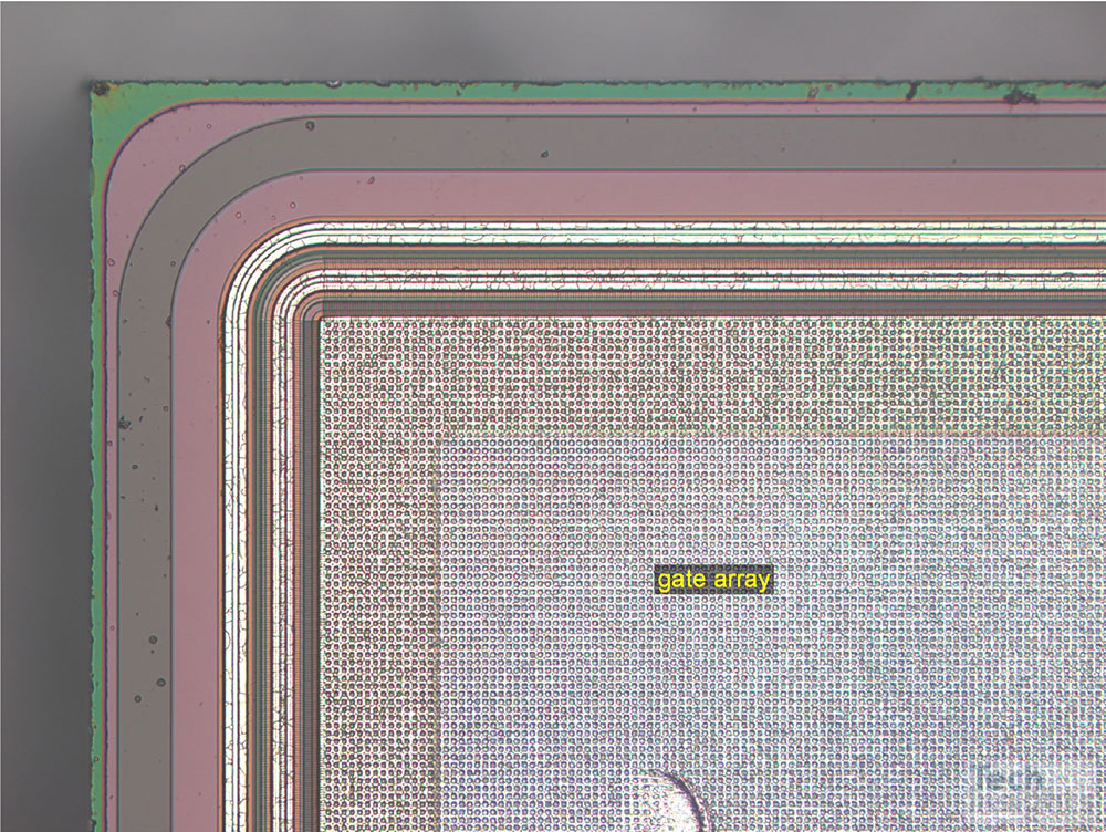
图1 SCT3022ALGC11 SIC电源FET模具角
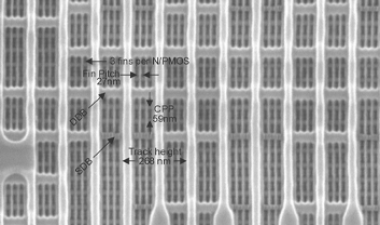
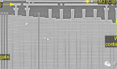
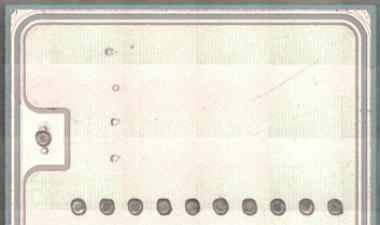
The layout of a single transistor cell of the SCT3022ALGC11 die at the polysilicon level can be seen in Figure 2. The square cell is comprised of a central body contact, surrounded by a dummy source trench gate. The active silicon region further surrounds the source trench. The active trench gate poly runs around the edge of each cell and is shared with adjacent cells. These active poly gates are connected electrically to the gate stringer at the edge of the array, shown in Figure 1. The transistor cell region was chosen for the process flow emulation since it represents the heart of the device.
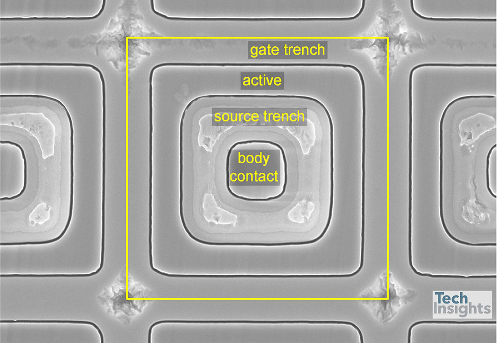
图2 Polysilicon的SCT3022ALGC11晶体管电池 - 平面图SEM
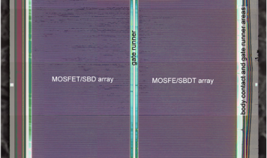
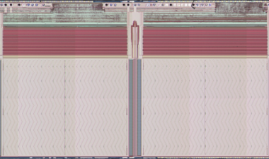
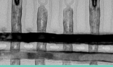
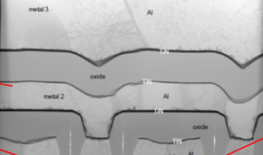
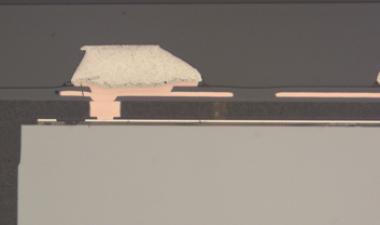
图3显示了穿过方形晶体管单元中间的横截面SEM图像。主体中央触点直接连接到顶部铝源金属。源/体接触区位于源沟附近,源沟也连接到源金属。有源栅沟位于单元边缘周围,如上图2所示。
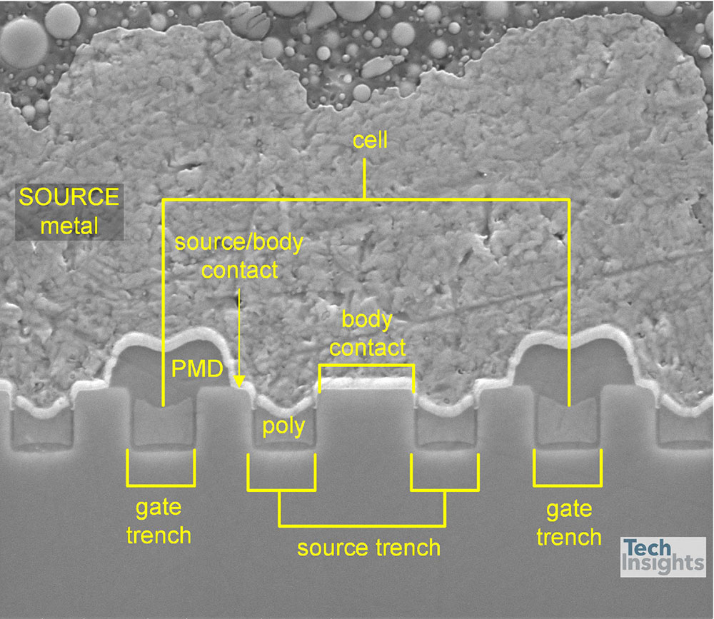
图3 SCT3022ALGC11晶体管单元-横截面SEM
其他显著特征需要更先进的分析技术。SCM是一种扫描探针技术,能够描绘半导体结构的掺杂区域。图4显示了穿过晶体管单元中间、以有源晶体管沟道栅极为中心的横截面相位对比度SCM图像。相衬SCM对掺杂类型敏感,P型材料给出正(蓝紫色)响应,N型材料给出负(黄色)响应。SCM显示有源沟道栅极由N型多晶硅形成,并且N+源区位于沟道栅极两侧附近。P+体区域似乎围绕假源沟道的底部延伸,并在有源栅的每一侧形成垂直沟道区域。这些掺杂区域将使用掺杂剂植入工艺形成。
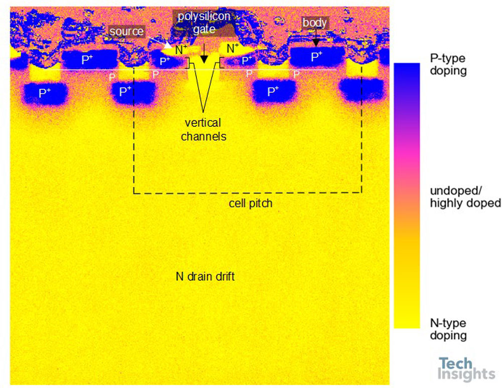
Figure 4 SCT3022ALGC11 Transistors Cell - Cross-Section SCM
TechInsights.analysts interpreted the structural, materials and dopant analysis described above to build a model of the steps taken during the device process flow. The data can then be used in conjunction with the the Synopsis森塔鲁斯过程资源管理器模拟过程流程。具体地,我们的逆向工程的详细结果用于制表SCT3022ALGC11模具的制造中使用的raybet正规么可能的过程步骤。基于对设备的每层的平面图成像的检查,以GDSII格式生成估计的掩模布局。图5显示了由处理仿真产生的晶体管电池区域的最终结构。图6中提出了一种示出了导致该最终结构的处理步骤的视频。
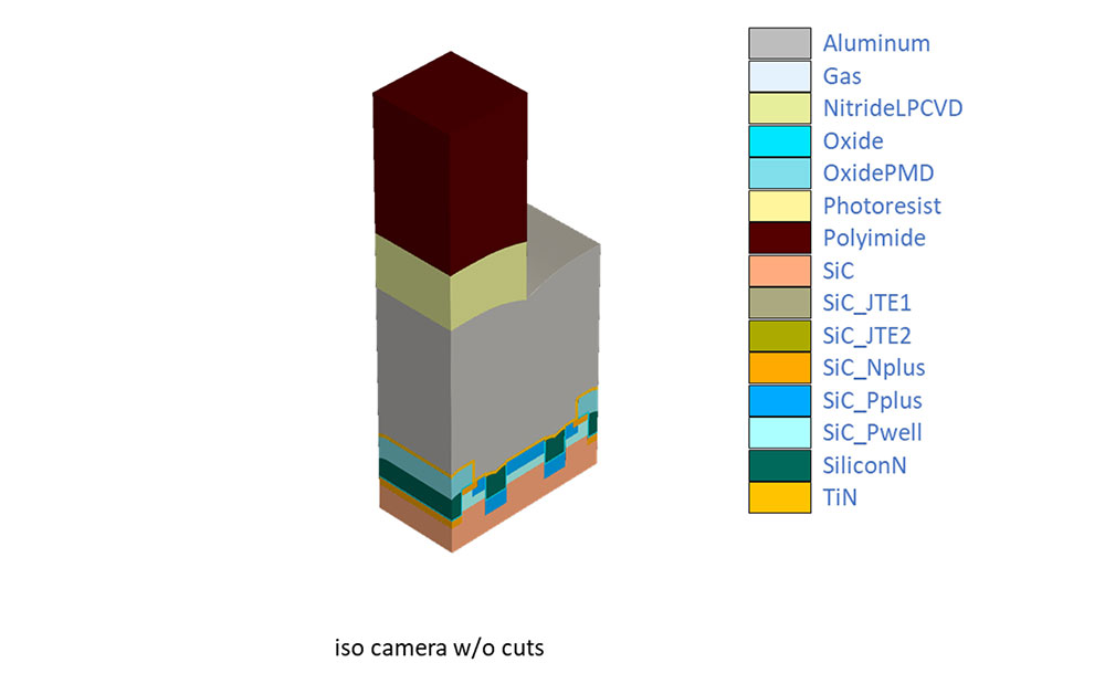
图5 SCT3022ALGC11过程仿真最终结构
图6 SCT3022ALGC11 Process Explorer仿真概要
过程flow analysis is a value-add process reverse engineering service that delivers greater insights through interpretation of the structural information provided by plan-view and cross-sectional analysis of the device’s structure. TechInsights is now offering this service to subscription clients across several technology verticals, including Power Semiconductor, Image Sensor, Memory, and Logic.